Uart Pcb Layout Guidelines
If your component placement forces horizontal trace routing on one side of the board, then always route traces vertically on the opposite side. 3) minimize the use of vias.

Uart Pcb Layout Guidelines PCB Circuits
Please follow the guidelines below for best results.
Uart pcb layout guidelines. This application note provides pcb layout guidelines for the rs9116 b00 sip module. 10 | page 6 uart layout guidelines the guidelines below must be followed for uart signals. Table 2.1 and 2.2 show the samples pcb stack up for 4 layers and 6 layers.
An_146 usb hardware design guidelines for ftdi ics version 1.1 document reference no.: Printed circuit board layout guidelines www.cypress.com document no. Use the import/export idf command in the pcb tool to reduce outline creation problems such as special shapes or a large number of holes.
Uart serial ports are widely adopted in huawei modules. Add label and packing 2016/06/08 1.2 1. To achieve the best overall system performance, please follow the guidelines specified in this document for circuit design and pcb layout.
5.2 power and ground planes the sections below describe typical 2, 4 and 6 layer board stackups. Rs9116 cc1 board layout guidelines version 1.1 silabs.com | building a more connected world. Keep the uart signals away from noisy sources or other sensitive signals.
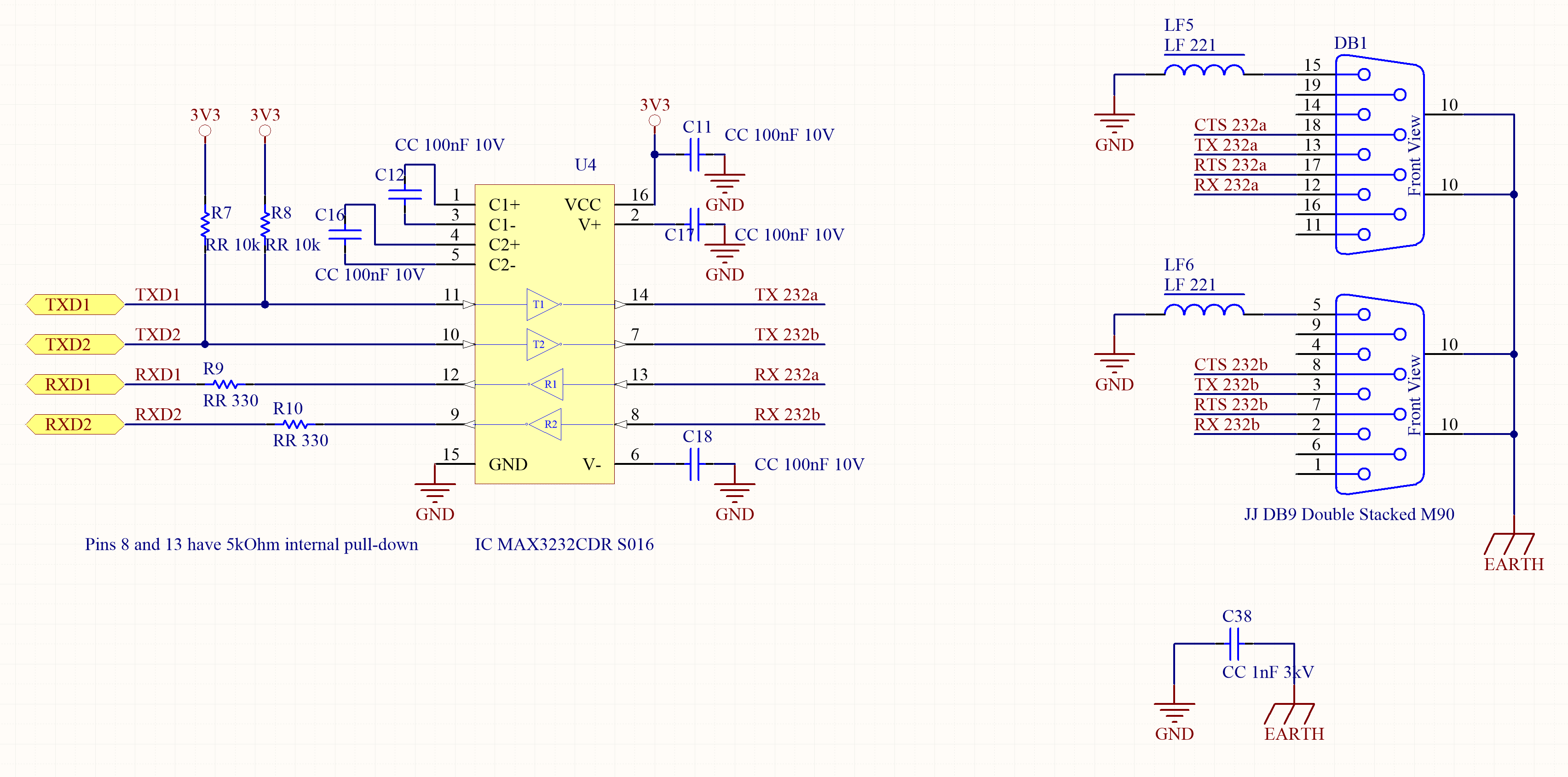
Add caution in gnss layout guide Espressif systems 7 esp32 hardware design guidelines v1.9. The signals are uart1_tx, uart1_rx, uart1_rts, uart1_cts.
Update pad and via design suggestion 3. While the high level of integration makes the pcb design and layout process simple, the performance of the system strongly depends on system design aspects. Add table1 for module wireless technology support overview;
Design guide v1.1 2 revision history rev date notes 0.1 jan 29, 2016 initial release 1.0 march 2nd, 2016 first release 1.1 sep 9, 2016 change uart, i2s and sdio to 3.3v These guidelines cover parts placement, various critical traces routing like rf, host interfaces routing like sdio/spi, usb, uart, power routing, and gnd pour. The goal of the 4 layer
2) place the buck circuit components on the same layer as the mcu. Add i/o default setting table as table 4; Cyw43439 pcb layout guidelines cyw43439 chip information 1.5 device description cyw43439 integrates the following on a single die:
2.3 number of pcb layers at least 4 layers are necessary, and 6 layers are recommended. 1) inductors and capacitors for the buck circuit should be placed as close to the mcu as possible. Communications through universal asynchronous receiver/transmitter (uart) serial ports is convenient and reliable.
4) traces for the buck circuit should be as thick as possible. 3 schematic checklist and pcb layout design 15 3.1 schematic checklist 15 3.1.1 power supply 16. The outline is the size and shape of the board.
This design guide describes the serial port specifications of huawei modules and provides recommended design schemes for peripheral circuits. Baseboard design and layout guidelines 090 technexion 10 5 baseboard pcb 5.1 pcb stackup recommendations it is recommended to use a 4 layer pcb for the baseboard with a thickness of 1.6 mm and 60 ohm (ω) impedance. Add notes to reserve test points on page16.
The size of the printed circuit board is very small, and the location of the components becomes a real challenge (especially when you come across a high speed interface layout). This command can decrease the time for outline creation and increase accuracy of the outline drawing. Pcb layout best practices recommend that you always place short, direct traces between components when possible, although this may not always be practical in larger boards.
When making determinations about part placement on the pcb, the following requirements must be met: Add gnss support in modem mode 2. Ftdi# 160 2 usb hardware design practices 2.1 trace style (matched pair, controlled impedance, length) usb requires two signals to make a single connection.
When laying out a printed circuit board (pcb) for the twl1200, careful consideration of design rules and guidelines must be employed to help preserve signal integrity and. To sum up, high speed pcb design is applied to devices with pcbs working at high frequencies with the use of high speed interfaces. All the common rules associated.
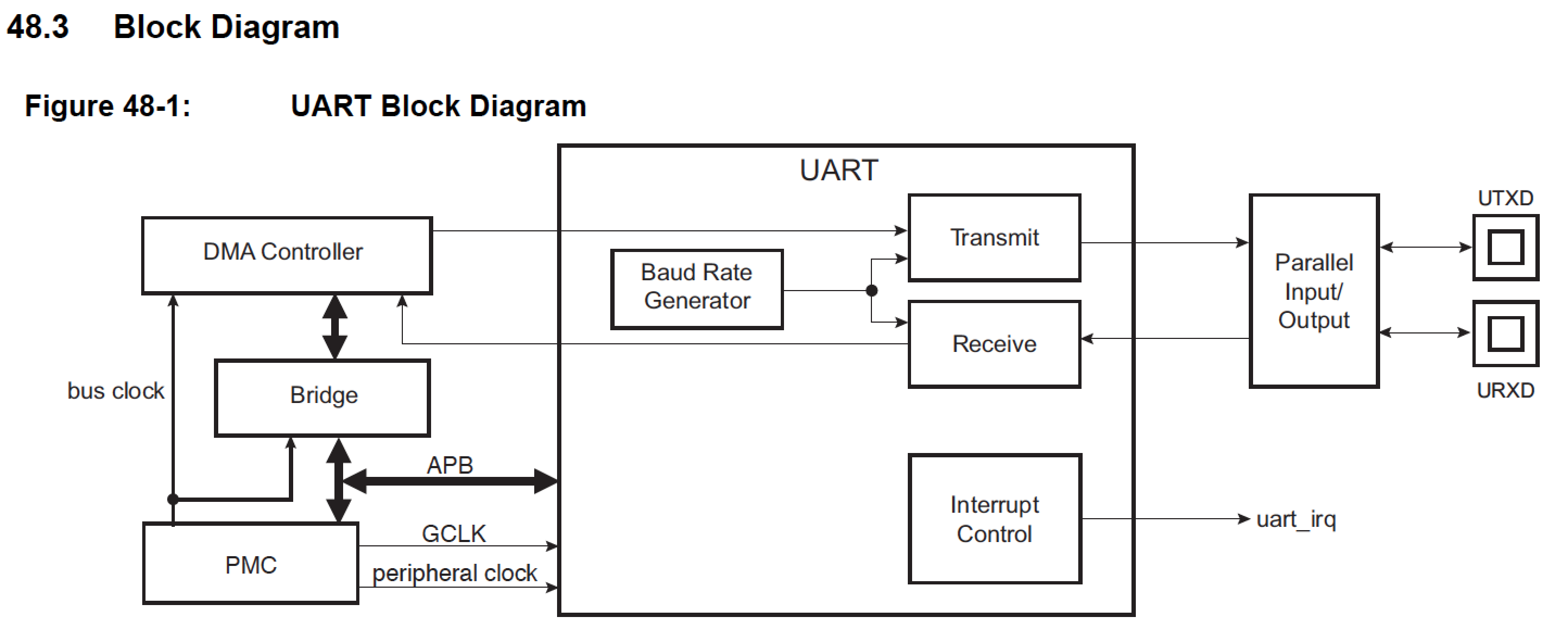
2.6 uart 13 2.7 adc 13 2.8 strappingpins 13 2.9 usb 15 2.10 touchsensor 16 3 pcb layout design 17 3.1 generalprinciplesofpcblayout 17 3.2 positioningamoduleonabaseboard 18 3.3 powersupply 20 3.4 crystaloscillator 21 3.5 rf 22 3.6 flashandpsram 24 For most data transfers, when one is high, the other is low.

Uart Pcb Layout Guidelines PCB Circuits

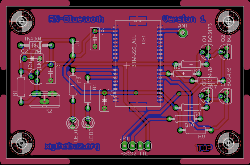
USB to UART Converter using Microchip MCP2200 PCB Design
dsPIC30F4011 Development Board


Never Mistake in pcb design Guidelines YouTube

General PCB Design and Layout Guidelines
UART Between Microcontrollers Using Proteus RS232
ACM041A, OLED UART Graphic, UART OLED MODULE, OLED UART

pcb USBUART Converter Design based on CH340G not

Basic PCB design rules that you must follow to make error
pcb Reference circuit design for UART on GSM module

Usb Type C Pcb Layout PCB Designs

Considerations in PCB layout guidelines Electrical
Uart Pcb Layout Guidelines PCB Circuits
Uart Pcb Layout Guidelines PCB Circuits
pcb design UART Floating Voltage on Custom PCB

RF PCB Venture Elctronics
[Resolved] [FAQ] PCB Layout Guidelines and Grounding
How to design the serial circuitry
SMPS PCB Layout Guidelines in Altium Designer